Key Features
- Wafer process and bumping in consolidated assembly.
- Technology supporting wide range of products from low-end applications such as mobile devices and digital electric household appliances to high-end applications such as servers.
- Promote multi-pin with min. 50µm AL pad pitch.
- Able to form wiring layer under a bump on demand.
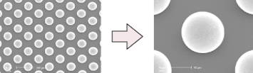
Bump external view
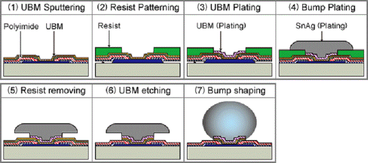
Manufacturing process
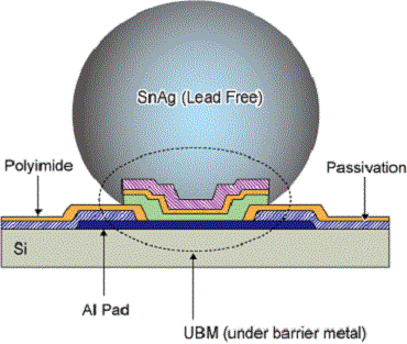
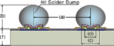
Bump cross section
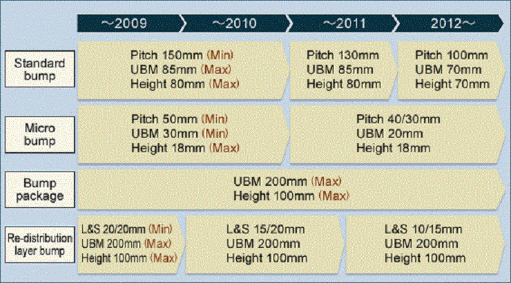
Technology road map
Mass-production actual results
| Wafer bumping | A | B | C |
|---|---|---|---|
| Purpose | High-end video | 1seg tuner | Image processing |
| Wafer size | 300 mm | 300 mm | 300 mm |
| Chip size | 9.52 × 14.44 mm | 2.90 × 2.90 mm | 5.10 × 4.50 mm |
| UBM size | 0.080 mm | 0.080 mm | 0.200 mm |
| Bump height | 0.085 mm | 0.085 mm | 0.100 mm |
| Bump pitch | 0.176 mm | 0.250 mm | 0.400 mm |
| Chip thickness | 0.550 mm | 0.185 mm | 0.450 mm |
| Bump material | SnAg | SnAg | SnAg |
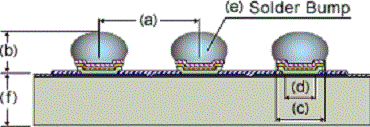
Typical specification
| (a) | Bump pitch | 176µm |
|---|---|---|
| (b) | Bump height | 85µm |
| (c) | UBM size | 80µm (typical) |
| (d) | Passivation opening size | 50µm (typical) |
| (e) | Bump material | SnAg (or PbSn) |
| (f) | Chip thickness (the thinnest case) |
200µm |
Micro bump chip specification (example)
| (a) | Bump pitch | 50µm |
|---|---|---|
| (b) | Bump height | 18µm |
| (c) | UBM size | 32µm (typical) |
| (d) | Passivation opening size | 17µm (typical) |
| (e) | Bump material | SnAg |
| (f) | Chip thickness (the thinnest case) |
150µm |